- 您现在的位置:买卖IC网 > Sheet目录1905 > ATMEGA32M1-AUR (Atmel)IC MPU AVR 32K 20MHZ 32TQFP
9397 750 14965
Koninklijke Philips Electronics N.V. 2005. All rights reserved.
Product data sheet
Rev. 02 — 20 June 2005
10 of 58
Philips Semiconductors
SC16C654B/654DB
5 V, 3.3 V and 2.5 V quad UART, 5 Mbit/s (max.) with 64-byte FIFOs
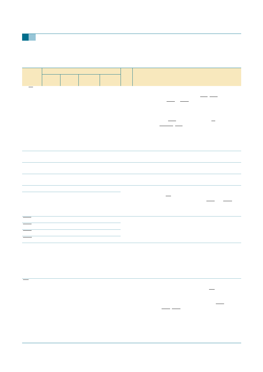
5.2 Pin description
Table 2:
Pin description
Symbol
Pin
Type Description
PLCC68 LQFP64 HVQFN48 LFBGA6
4
16/68
31
-
14
-
I
16/68 Interface type select (input with internal pull-up).
This input provides the 16 (Intel) or 68 (Motorola) bus
interface type select. The functions of IOR, IOW,
INTA to INTD, and CSA to CSD are re-assigned with the
logical state of this pin. When this pin is a logic 1, the
16 mode interface (16C654) is selected. When this pin is a
logic 0, the 68 mode interface (68C654) is selected. When
this pin is a logic 0, IOW is re-assigned to R/W, RESET is
re-assigned to RESET, IOR is not used, and INTA to INTD
are connected in a wire-OR conguration. The wire-OR
outputs are connected internally to the open-drain IRQ
signal output. This pin is not available on 64-pin packages
which operate in the 16 mode only.
A0
34
24
17
K5
I
Address 0 select bit. Internal registers address selection in
16 and 68 modes.
A1
33
23
16
J5
I
Address 1 select bit. Internal registers address selection in
16 and 68 modes.
A2
32
22
15
K4
I
Address 2 select bit. Internal registers address selection in
16 and 68 modes.
A3
20
-
9
-
I
Address 3, Address 4 select bits. When the 68 mode is
selected, these pins are used to address or select individual
UARTs (providing CS is a logic 0). In the 16 mode, these
pins are re-assigned as chip selects, see CSB and CSC.
These pins are not available on 64-pin packages which
operate in the 16 mode only.
A4
50
-
31
-
CDA9
64
-
A1
I
Carrier Detect (active LOW). These inputs are associated
with individual UART channels A through D. A logic 0 on this
pin indicates that a carrier has been detected by the modem
for that channel.
CDB
27
18
-
K2
CDC
43
31
24
J9
CDD
61
49
-
A10
CLKSEL
30
-
I
Clock Select. The 1
× or 4× pre-scalable clock is selected by
this pin. The 1
× clock is selected when CLKSEL is a logic 1
(connected to VCC) or the 4× is selected when CLKSEL is a
logic 0 (connected to GND). MCR[7] can override the state
of this pin following reset or initialization (see MCR[7]). This
pin is not available on 64-pin packages which provide
MCR[7] selection only.
CS
16
-
5
-
I
Chip Select (active LOW). In the 68 mode, this pin
functions as a multiple channel chip enable. In this case, all
four UARTs (A to D) are enabled when the CS pin is a
logic 0. An individual UART channel is selected by the data
contents of address bits A[3:4]. when the 16 mode is
selected (68-pin devices), this pin functions as CSA (see
denition under CSA, CSB). This pin is not available on
64-pin packages which operate in the 16 mode only.
发布紧急采购,3分钟左右您将得到回复。
相关PDF资料
ATMEGA48PA-MMNR
MCU AVR 4KB FLASH 20MHZ 28QFN
ATMEGA644P-B15MZ
IC MCU 8BIT 64KB FLASH 32VQFN
ATMEGA644V-10PU
IC AVR MCU FLASH 64K 40DIP
ATMEGA645V-8MI
IC AVR MCU FLASH 64K 1.8V 64QFN
ATMEGA649-16MI
IC AVR MCU FLASH 64K 5V 64QFN
ATMEGA649V-8MI
IC AVR MCU FLASH 64K 1.8V 64QFN
ATMEGA8515L-8JUR
MCU AVR 8KB FLASH 8MHZ 44PLCC
ATMEGA8515L-8PJ
IC MCU AVR 8K 5V 8MHZ 40-DIP
相关代理商/技术参数
ATMEGA32M1-MU
功能描述:8位微控制器 -MCU 32KB FLASH 1KB EE 2KB SRAM 20 MHz 5V RoHS:否 制造商:Silicon Labs 核心:8051 处理器系列:C8051F39x 数据总线宽度:8 bit 最大时钟频率:50 MHz 程序存储器大小:16 KB 数据 RAM 大小:1 KB 片上 ADC:Yes 工作电源电压:1.8 V to 3.6 V 工作温度范围:- 40 C to + 105 C 封装 / 箱体:QFN-20 安装风格:SMD/SMT
ATMEGA32U2
制造商:ATMEL 制造商全称:ATMEL Corporation 功能描述:8-bit Microcontroller with 8/16/32K Bytes of ISP Flash and USB Controller
ATMEGA32U2-AU
功能描述:8位微控制器 -MCU USB 32K FLASH RoHS:否 制造商:Silicon Labs 核心:8051 处理器系列:C8051F39x 数据总线宽度:8 bit 最大时钟频率:50 MHz 程序存储器大小:16 KB 数据 RAM 大小:1 KB 片上 ADC:Yes 工作电源电压:1.8 V to 3.6 V 工作温度范围:- 40 C to + 105 C 封装 / 箱体:QFN-20 安装风格:SMD/SMT
ATMEGA32U2-AUR
功能描述:8位微控制器 -MCU USB 32K FLASH 16 MHz RoHS:否 制造商:Silicon Labs 核心:8051 处理器系列:C8051F39x 数据总线宽度:8 bit 最大时钟频率:50 MHz 程序存储器大小:16 KB 数据 RAM 大小:1 KB 片上 ADC:Yes 工作电源电压:1.8 V to 3.6 V 工作温度范围:- 40 C to + 105 C 封装 / 箱体:QFN-20 安装风格:SMD/SMT
ATMEGA32U2-MU
功能描述:8位微控制器 -MCU AVR USB 32K FLASH INDUSTRIAL RoHS:否 制造商:Silicon Labs 核心:8051 处理器系列:C8051F39x 数据总线宽度:8 bit 最大时钟频率:50 MHz 程序存储器大小:16 KB 数据 RAM 大小:1 KB 片上 ADC:Yes 工作电源电压:1.8 V to 3.6 V 工作温度范围:- 40 C to + 105 C 封装 / 箱体:QFN-20 安装风格:SMD/SMT
ATMEGA32U2-MUR
功能描述:8位微控制器 -MCU USB 32K FLASH 16 MHz RoHS:否 制造商:Silicon Labs 核心:8051 处理器系列:C8051F39x 数据总线宽度:8 bit 最大时钟频率:50 MHz 程序存储器大小:16 KB 数据 RAM 大小:1 KB 片上 ADC:Yes 工作电源电压:1.8 V to 3.6 V 工作温度范围:- 40 C to + 105 C 封装 / 箱体:QFN-20 安装风格:SMD/SMT
ATMEGA32U4
制造商:ATMEL 制造商全称:ATMEL Corporation 功能描述:8-bit Microcontroller with 16/32K Bytes of ISP Flash and USB Controller
ATMEGA32U4-16AU
功能描述:8位微控制器 -MCU 32K Flash
RoHS:否 制造商:Silicon Labs 核心:8051 处理器系列:C8051F39x 数据总线宽度:8 bit 最大时钟频率:50 MHz 程序存储器大小:16 KB 数据 RAM 大小:1 KB 片上 ADC:Yes 工作电源电压:1.8 V to 3.6 V 工作温度范围:- 40 C to + 105 C 封装 / 箱体:QFN-20 安装风格:SMD/SMT